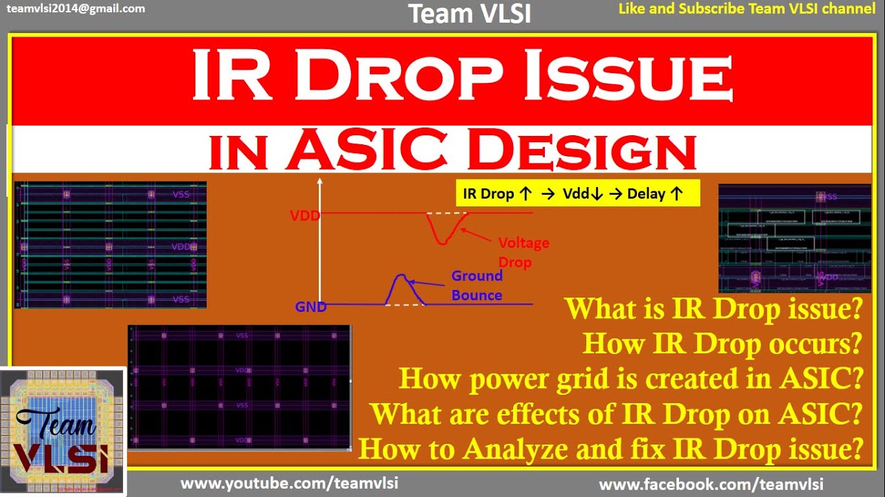
This Drop is called as IR Drop. IR drop while causing an increase in delay for a digital transistor can have an even bigger impact on analog circuitry.

Team Vlsi Ir Drop Analysis In Physical Design Ir Analysis In Vlsi
Welcome to our site.

. Vlsi pnr cts physicaldesign mtech cadence synopsys mentor placement floorplan routing signoff asic lec timing primetime ir electromigratio. Some voltage will drop due to the resistance. First a fast model with some extend of accuracy is proposed to quantify the IR-drop of a block.
However IR-drop analysis usually takes a long time and wastes so many resources. The vulnerability of power and clock signal interconnects to EM is more in high-density IC packages. How Did You Do Cts For The Same.
Click here to register now. In this situation the voltage will be lost due to the Ohms law. Design current requirement Width of power meshes.
IR Drop and EM Analysis IR Drop Drop happens in supply voltage when traverses through the power network. Physical information of the design report_design_physical Digital Signal Processing Tutorial. For example a design needs to operate at 2 volts and has a tolerance of 04 volts on either side we need to ensure that the voltage across its power pin Vdd and ground pin Vss in that design does not fall short of 16 VoltsThe acceptable IR drop in this context is 04 volts.
Use MIM Metal -Insulator Metal for stabilizing the power Q215. Since IR-drop leads to lower instantaneous supply. I had 5 clocks in my designs sys_clk sys_rclk uart_clk g_clk and scan_clk where sys_clk g_clk and uart_clk logically exclusive to.
Power requirement of the design Power network structure. IR core 775 mV IR package IR pads 5 To determine values for IRpackage and IRpads consider that IRpackage consists of two components. Designs approach to 90nm and deeper the problem caused by IR-drop has become one of the top culprits of defects 7.
Q 27What is IR drop. Increases skew Use different power grid tap points for clock buffers but it makes routing more complicated for automated tools Use smaller buffers but it degrades edge ratesincreases delay Rearrange blocks More VDD pins Connect bottom. In this paper IR-drop constraint is considered in floorplanning stage in order to solve problem in the early stages of physical design and shorten time to market.
Electro Migration EM Current density checks on power network Depends on. Not only can timing change but it can directly cause functional failures. The engineers perform post-layout static timing analysis STA and feed the results into an IR-drop analysis engine.
Package cross-section showing IR drop components Combining 3 4 and the value for IR chip found in 2 provides a formula for determining an actionable IR drop target for the physical design process. This drop in voltage is known as the IR drop. To participate you need to register.
Amount of current drawn from the power grid is directly proportional to the output capacitance thats being driven. IR drop is a voltage drop which affects technology node performance. Given that the current draw of a wire is influenced by activity in other areas of the chip it is often seen as a source of noise for the analog circuitry and this has to be taken into account.
During design signoff power integrity analysis and fixing are available in the physical design step to help block-level and top-level engineers converge. We cant have functional failure in our design. Industry standard Project Execution 1.
Each metal layer has a resistance valueWhen the current flows through the metal the resistance consumes some currentThis is the IR dropIf the resistance is more the drop. In this work we develop a fast dynamic IR-drop predictor based on a. Load splitting can reduce the peak current demand from the power grid.
IR Drop Intensifies in the Presence of EM With the decrease in the device dimensions there is speed and current density shoot up in VLSI systems. How Many Clocks You Had In Your Designs. Physical verification is the process of ensuring a designs.
Current I Increases near inductor so L dIdt increases due to which Voltage drop across Inductor increases hence less voltage at the partition or logic group or registers is seen in the design. And then selection strategy in. And a whole lot more.
Remedies Stagger the firing of buffers bad idea. Suffer more seriously IR-drop problem. Physical Design The physical design process produces a set of layout files which describe the position of cells and routes for the interconnections between them.
So dynamic IR drop will be addressed. IR-drop is a fundamental constraint by almost all integrated circuits ICs physical designs and many iterations of timing engineer change order ECO IR-drop ECO or other ECO are needed before design signoff. There are two types of IR drops.
By using IR-A TA the impact of physical design changes that control or suppress the voltage drop or voltage variation could be quanti ed and the resulting. Energy is converted from electrical energy into thermal energy and the value for the voltage also decreases. IR Drop in PCB Design Voltage is connected to the device pin via a plane or trace which has resistance and is known as IR drop on PCBs.
So to avoid any kind of functional failure due to Dynamic IR we use Decap cells in our design.

Vlsi Basics Electromigration Ir Drop
Team Vlsi Ir Drop Analysis In Physical Design Ir Analysis In Vlsi

Vlsi Soc Design Ir Drop Analysis Ii

Vlsi Soc Design Ir Drop Analysis Ii
Ir Drop Issue In Vlsi What Is Ir Drop In Asic Why Ir Drop Effects Of Ir Drop Youtube

Vlsi Soc Design Ir Drop Analysis Ii

Vlsi Soc Design Ir Drop Analysis Ii

Team Vlsi Ir Drop Analysis In Physical Design Ir Analysis In Vlsi
0 comments
Post a Comment